These arise from the extension of transistor fabrication techniques to the assembly of complex electronic circuits on a single silicon chip. Thus most low-power stages used in receivers and transmitters, such as amplifiers (RF, IF and AF), demodulators, oscillators, stabilizers etc. are available as a single device. Few peripheral discrete components are required. Thus equipment has become smaller and more complex with extra facilities, and at the same time more reliable.
The most common way to refer to integrated circuits (IC's), is by the name 'chip' or 'chips'. The name chip is the derived from the name of the tiny piece of silicon, which is at the very centre of each package. A large circular wafer containing many silicon chips is made, then individual chips are 'chipped' or cut away from the wafer.
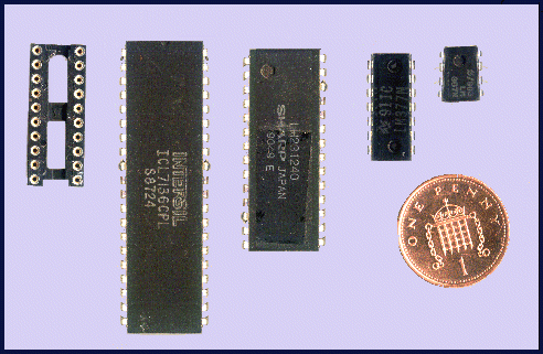
The chip can contain may thousands of transistors, resistors, and capacitors, mass manufactured in a microscopic circuit etched within the tiny chip of silicon. Almost invisible gold wires then link the actual chip to outside world, via the pins (or legs) of the IC. The pins are numbered up from 1, starting with pin 1 in the top left hand corner, counting clockwise around the whole IC. A notch in the package of each IC (just visible in the photo) denotes the end of the chip nearest pin 1.
For ease of repair, or if the IC contains software which may from time to time require updating, the IC may be mounted in a socket, rather than being soldered to the PCB (Printed Circuit Board).
Photo 3.4. An IC socket (left) and a selection of integrated circuits. Chips like these may contain many thousands (or millions) of components etched into its silicon chip.
Looking at the photograph of the integrated circuit below, in the middle of the package is a tiny circular quartz window with a tiny silver object at the centre. The silver object is the actual chip itself, based on a gold coloured base. The chip is an EPROM (Erasable Programmable Read-Only Memory). It is programmed with software, and may be erased for reprogramming by exposing the chip to ultra-violet light. The window is usually covered after programming to prevent accidental erasure of the software. In the magnified view of the window (right) you can see the chip and even the gold wires connecting the pins to the silicon.
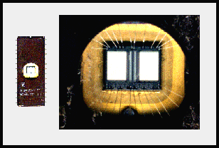
Photo 3.5 An EPROM IC (left) and a close up of the quartz window (right) The fine lines are the gold wires inter-connecting the pins of the IC package to the silicon chip itself. The two white oblongs shapes are approximately 2mm wide.
Older more traditional construction methods, where components had wire 'legs', have been replaced by surface mounted components, especially so in commercial equipment. Instead of the legs passing through holes in the printed circuit board (PCB), the components are simply laid on the PCB onto solder pads, which are then soldered in place. This has given rise to much smaller components and much more compact PCB's. Typical PCB sizes are now a around 70% smaller than was possible with through the PCB mounting of components. Most of the traditional wire leaded components can now be obtained in SM versions.
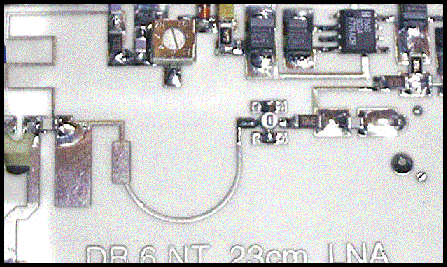
Photo 3.5. A typical radio amateur produced surface mount PCB (23cms Low Noise Amplifier).
The two similar black items (close to the upper edge of the photo, and right of centre), are SM diodes, with a SM IC to the right of these.