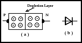
A diode consists of a small single piece of silicon or germanium in which one end has been made N-type and the other P-type. Because the two ends of the material have different characteristics as described above, there is a diffusion of holes in one direction and electrons in the other. This forms an area where electrons will have jumped into vacant holes and a boundary or junction formed stopping any further migration of holes and electrons as shown diagrammatically in Fig 3.2. This area is known as the depletion layer'. This layer is typically 0.001mm in thickness.
Fig 3.2. The junction diode
The depletion layer has formed a region where work must be done to get further electron/hole movement, ie energy must be provided externally. This can be provided in the form of a voltage from, say, a battery.
Consider the circuit of Fig 3.3 with the polarity of the battery as shown. The electrons from the N-region will be attracted by the positive plate of the battery and so will be assisted to cross the depletion layer. This will then leave holes in the N-region which are filled by electrons entering from the wire conductor and the rest of the circuit by a chain reaction. The electrons that enter the P-region will be pulled into the wire due to this chain reaction. Thus a conventional current flows (note that conventional current flow is in a direction opposite to that of electron flow). This condition is known as 'forward bias'.
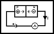
Fig 3.3. The forward-biased junction diode
If the polarity of the battery is reversed it is found that the electrons accumulate at the battery end of the N-region and similarly for the holes in the P-region.
Thus negligible current flows. This is known as 'reverse bias'. The device that has been formed is known as a 'diode' (or 'rectifier'). It allows current to flow in only one direction and this is determined by an externally applied voltage. In the forward bias condition it is found that no current flows until a certain voltage has been applied across the diode (called the 'barrier potential'). With germanium this is found to be about O.3V and with silicon about 0.6V. This corresponds to the work that must be done in helping the electron to cross the depletion layer. The depletion layer becomes narrower with increased forward bias. Note that whenever current flows, this voltage appears across the diode.
This property of the PN junction can be described by the graphs in Fig 3.4. A small current is found to flow under reverse bias conditions and increases with temperature. This is much more marked in germanium diodes than silicon diodes. This current is known as 'leakage current'. Please note the change in scale, between positive and negative, of the vertical axes.
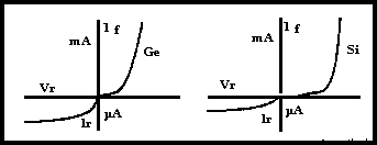
Fig 3.4 Characteristics of germanium and silicon diodes
This basic diode is used for the rectification of alternating voltages in power supplies, demodulating signals in radio receivers and certain logic functions. The type of diode for an application will depend on current, maximum reverse voltage to be expected and frequency.
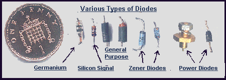
Photo 3.1 A Selection of diodes
By changes in the manufacturing process. diodes can be made to exhibit somewhat different characteristics. Three of these - the zener diode, the variable capacitance diode and the light-emitting diode are examined next.