Small-signal amplifiers are so called because their inputs are usually in the microvolt or millivolt range as opposed to large signal amplifiers which have inputs of the order of volts. The latter are normally referred to as 'power' amplifiers; these are dealt with later. Whichever type, the base, emitter and collector of the transistor must be set to various DC voltages so that it will act as an amplifier. This setting up of DC conditions is known as 'biasing' and if incorrectly chosen, the amplifier may distort the signal. Amplifiers can be used for DC, through AF, up to RF and microwaves. Only AF and RF types are considered here.
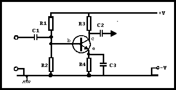
Fig 3.19 shows a typical common-emitter circuit and represents the most widely used of the amplifiers. Capacitors C1 and C2 provide AC coupling into and out of the circuit respectively. R1 and R2 provide biasing (note that this is not the only method of biasing but is the most stable). R3 is the collector load while R4 helps set up the DC bias conditions with C3 (the emitter bypass capacitor) acting as an AC short circuit across it. With C3 acting as an AC short-circuit (ie its reactance is very small at the operating frequency), the emitter, as far as the AC is concerned, appears the same as the 0V line and is thus common to input and output signals. This gives the amplifier its name.
Fig 3.19. Typical common-emitter amplifier
The values of C1, C2 and C3 are chosen so that they have very low reactance at the operating frequency. Their value will therefore vary according to the frequency being amplified; at audio they may be electrolytic capacitors, while at RF they may be in the l000pF range or less. The biasing of the transistor has to be carefully chosen so that minimum distortion will occur of the signal being amplified. The voltage of the base must be about 0.6V above the emitter (assuming a silicon transistor). This allows a standing bias current through the transistor determined by R4. Knowing this value means the standing (or quiescent) voltage of the collector is known. Fig 3.20 shows the effect of too high and too low a voltage at the collector. In cases (a) and (b) distortion occurs which manifests itself as harmonics. Case (a) is when the input voltage cannot maintain the 0.6V differential between the base and emitter and has effectively caused zero collector current; the transistor is 'switched off'.
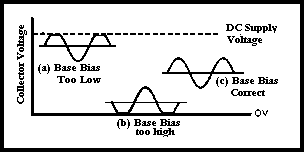
Fig 3.20. Effects of base bias on the collector voltage
The operation of a common-emitter circuit is as follows. Assuming the input voltage at the base is converted to a base current, then if the input voltage increases, so does the base current. This causes an increase in collector current and because one end of R3 is attached to +V, then for increased current the voltage across R3 must increase and so the voltage at the collector decreases. If the input voltage decreases, then so does the base current and hence the collector current. This causes less current through R3 and so the collector voltage rises. It should be noted that the collector voltage does the opposite to the input voltage, ie it is out of phase or inverted (ie 180°). Typical values for R1, R2, R3 and R4 might be 27kΩ, 8.2kΩ, 4.7kΩ and 1.5kΩ respectively.
One aspect not yet considered is how one circuit is affected by another one connected to it. For example, if one common-emitter amplifier cannot give enough gain then it can be followed by a second one in series. All electronics are the effective connection of a series of basic building blocks. The second circuit obviously must take a signal from the first one and this leads to the question of how one circuit 'loads' another. This is commonly expressed by the concept of input and output impedance's.
Ideally the input resistance should be high so that it does not load a previous circuit too much and the output resistance should be reasonably low so that most of the output voltage can be passed to the next circuit.
For a typical common-emitter amplifier the input resistance is between 500Ω and 2kΩ and the output resistance between 5 and 20kΩ but the circuit resistors do have some effect on these figures. The common-emitter amplifier does not always represent an ideal arrangement and there are two other transistor configurations to consider - the common-collector (or emitter-follower) and common-base circuits.
The name in brackets for this is the most popular, but the first one follows a logical sequence. It may also be referred to as a 'buffer'. Fig 3.21 shows a typical circuit with values.
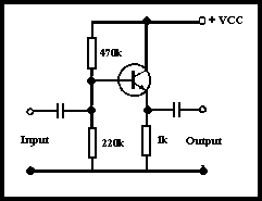
Fig 3.21. Typical emitter-follower circuit
If the input voltage increases in this circuit, the base current rises and hence the collector current. As the emitter current is almost the same as the collector current, then the current through the emitter rises and hence the voltage at the emitter rises (one end of R3 is fixed to 0V and cannot change). If the input voltage decreases then the emitter voltage must also decrease with like reasoning. Because the base is always 0.6V greater than the emitter, then the emitter voltage is always less than the base voltage; ie there is a voltage gain of less than unity. The input resistance of this circuit is about l00kΩ while the output resistance is maybe only 1kΩ (again, both are dependent on the effects of circuit resistors). This makes an ideal circuit in preventing loading of one circuit and feeding the next one with little voltage loss. It acts as a buffer between two circuits and hence its alternative description.
This is the third configuration and Fig 3.22 shows a typical arrangement. The signal is applied between base and emitter. If the input voltage increases, then the emitter voltage will rise and cause less of a differential between emitter and base. This means that the transistor takes less base current and so the collector current drops. This in turn causes a rise in collector voltage. If the input voltage drops then the reverse happens and the collector voltage drops. Hence, the collector voltage is in phase with the input voltage and so there is no phase inversion for voltage. The input impedance is very low, about 50-100KΩ, so it is easy to match to a transmission line and/or antenna system. The output resistance is very high (at least 50kΩ).
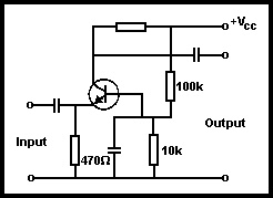
Fig 3.22. Typical common-base circuit
Table 3.1. Characteristics of transistor configurations
| Common emitter | Common collector | Common base | |
| R in | 1kΩ | 100kΩ | 50-100Ω |
| R out | 20kΩ | 1kΩ | 50kΩ |
| Current gain | 50 | 50 | 0.98 |
| Voltage gain | -100 | 0.98 | 100 |
Each of these circuits just discussed has its own specific properties as mentioned, and these are summarized in Table 3.1. It is stressed that these values are only typical as so much depends on other factors such as external resistors, transistor parameters and operating conditions. The negative sign in front of a gain figure shows that the output signal is out of phase with the input signal. Voltage gain of less than 1 indicates that the signal is reduced, or attenuated, by the amplifier.
As the frequencies in use rise, so the internal capacitance effects of the transistor must be taken into account and the word 'resistance' in the above discussion must be replaced by 'impedance'. Generally the input impedance gets lower and so does the output impedance. The value of the internal capacitance eventually has to be taken into account when designing adjacent circuitry but this is a matter beyond the present level of discussion.