The word 'transistor' must be treated carefully. It is in fact a word describing a family of devices but is often used to refer to the NPN and PNP type only. The NPN and PNP transistors are technically 'bipolar transistors'.
The transistor was discovered in 1947 and entered production in 1951. Early types were made from germanium but silicon has now surpassed them in most applications. It has also been fabricated in various forms, and names such as 'junction', 'epitaxial', 'planar' etc are common in data sheets. The basic operation is, however, the same, the different methods of fabrication offering different characteristics.
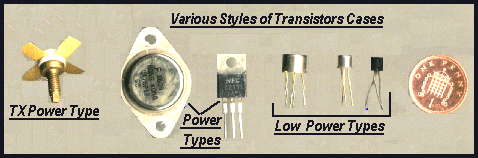
Photo 3.3 A selection of transistors
The device is made from a single piece of silicon (or germanium). The various regions are created chemically to give an NPN or PNP structure - that is two PN junctions (the NPN form being more common). It has three terminals known as 'collector', 'base' and 'emitter'. Fig 3.7 shows a typical NPN junction-type bipolar transistor. The device is 'current controlled', ie the base current controls the amount of current flowing between the collector and emitter. The higher the base current, the greater the current flow between collector and emitter and of course the converse.
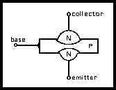
Fig 3.7. The NPN Transistor
To enable a bipolar transistor to function, the voltages of the collector, base and emitter must be correct with respect to one another - this is known as 'biasing'. The following discussion is for a silicon device as these are more common. Also, the description is for an NPN device - for a PNP type all voltages and currents are reversed. Fig 3.8 shows a very basic method of biasing; in reality only one power supply source would be used.
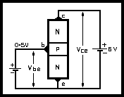
Fig 3.8. Biasing the transistor
From Fig 3.8 it can be seen that the base is 0.5V above the emitter, and this therefore forms a forward-biased PN junction. The collector is higher than the base voltage and so this forms a reverse-biased PN junction. A set of measurements could be carried out for various values of collector voltage, collector current, base voltage and base current and a set of curves would be obtained as shown in Fig 3.9. These are known as the 'characteristic curves' for that transistor. These are the graphs shown in transistor data sheets.
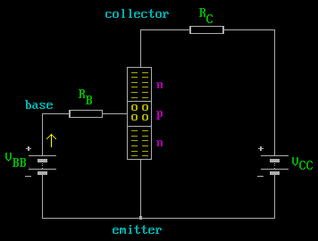
This animation shows the current flow in the circuit of Fig 3.8.
The current flow through the resistor in the collector (Rc), will be several times larger than that flowing through the resistor in the base (RB). Without the resistors in place, the transistor junctions in the above circuit would very quickly overheat and burn out.
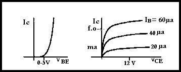
Fig 3.9. Characteristics of a small-signal transistor
There are various parameters available to describe a transistor. These can relate to voltage, current, power, gain, frequency and operating temperature; which of these are relevant depends on the application. The voltage rating gives an indication of the maximum voltages the transistor can withstand; the current will specify maximum currents the device can handle; and power, the maximum power the device can deliver to a load or dissipate itself. The gain is a relationship between input and expected output , the frequency will specify the range the device is capable of working over and the temperature how hot the device can run (this is also related to power). Transistors come in various shapes and sizes, usually depending on the current or power to be handled. Unfortunately there are subdivisions of the above which can make matters more complicated but some basic parameters are discussed below. The maximum collector voltage specifies, as the name suggests, the maximum voltage that the collector can withstand ,hence the DC power supply may help determine the choice of transistor.
The current gain relates the change of collector current with change of base current. If the collector current changes from 1 to 2mA when the base current changes from 5 to 10uA, then the current gain is 1mA/5uA = 200. The symbol for current gain is hfe or, mainly in older literature, B or β (the Greek letter "beta"). Depending on transistor type, current gains from 2 to 800 are possible. Values for silicon devices are higher than those for germanium. Note also, that hfe can vary significantly between samples of the same transistor type. It should therefore only be taken as a guide to the device's capabilities and not relied upon in actual design.
The transition frequency fT is the frequency at which the current gain of the device has fallen to unity. Transistors are normally used up to a value of 10-15% of this figure. There are no hard and fast rules as this depends on the application.
The power the device will handle is dependent on several factors: how efficient the particular circuit arrangement is, the output power wanted, the ambient temperature and the cooling available (heat sink, air circulation etc). Always run as cool as possible for reliability. A typical example of the advantage of a heat sink can be shown by considering a BFY50. This will dissipate 0.8W with no heat sink if the temperature can be kept below 25°C. With a given size heat sink, this could be extended to 100°C and a dissipation of 2.8W. It is the actual temperature of the chip, ie the small piece of silicon on which the transistor is assembled, that is of paramount importance.
Germanium transistors were developed before the silicon transistor but they tend to be much more affected by operating temperatures. For example, the maximum safe working temperature for a germanium device is about 75°C while for a silicon device it is about 150°C. Hence silicon devices are generally to be preferred.
The British Standards (BS) symbols for the two types of transistor are given in Fig 3.10. The arrow is always on the emitter.
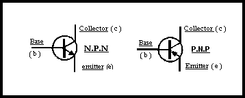
Fig 3.10. Transistor symbols