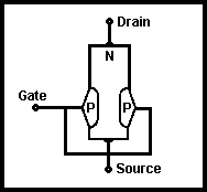
This is another member of the transistor family which is widely used and has advantages in certain applications. It comes in various forms: JFET, IGFET, MOSFET etc, but only the JFET (junction FET) will be described here. Both N-and P-types exist but the description of operation will be that of an N-channel type. Fig 3.11 shows the construction diagrammatically.
Fig 3.11. The field-effect transistor
It consists essentially of a P-type region diffused into an N-type channel. The P-type region, or 'gate', creates a junction with the N-type bar and hence a depletion layer. The main current flow is from drain to source, the voltage applied at the gate being used to control this current. Thus, the FET is a voltage-controlled device as opposed to the bipolar transistor which is current controlled (ie base current controls collector-emitter current)
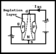
Fig 3.12. Configuration and operation of a FET
To operate, biasing is required (see Fig 3.12). This is shown with batteries but in reality only one DC supply would be used. This must make the gate negative with respect to the source and hence a reverse-biased PN junction, thus exhibiting high input resistance. The drain must be positive with respect to the source. By varying the voltage on the gate the depletion layer width can be varied - the more negative the voltage, the wider the depletion layer, and the less the drain-source current. The voltage required to reduce the drain current to zero is known as the 'pinch-off voltage'. A typical set of characteristics for a 2N3823 JFET is shown in Fig 3.13. The FET is a useful device as it always exhibits very high gate input resistance. The BS symbols for the types of JFET are given in Fig 3.14.
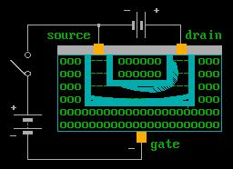
The above animation shows an FET in operation.
Typically FET's have an extremely high input impendence, and only tiny amounts of current are required to operate them. The voltage on your finger tip, will cause the gate to operate.
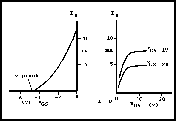
Fig 3.13. Characteristics of a 2N3823 FET
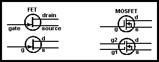
Fig 3.14. BS Symbols for various FETs
Generally it is only possible to distinguish an FET from a Bi-Polar transistor by its type number. The packages used are identical.